Sustainable Semiconductor Production with reduced environmental footprint and optimized parameters
The semiconductor industry aims to be CO2-neutral by 2040 in order to meet the goals of the Paris climate agreement and to be compliant with the supply chain law of transparent PCF (Product Carbon Footprint) between the companies. To achieve this, the CO2 footprint of processes and products must be known and be reduced in the long term. This requires a granular collection of relevant input and output key figures (raw material, energy and water) of the processes for the exact determination of the environmental impact of manufactured products in order to reduce CO2 emissions.
Therefore “Cluster 3 Sustainability” focuses on three relevant use cases:
- Development of a Life Cycle Assessment (LCA) methodology with the underlying Life Cycle Inventory (LCI): Data acquisition of environmentally relevant parameters along the vertical and horizontal supply chain in the semiconductor industry.
- Optimization of environmental key figures by statistical mathematical and AI methods: Reduction of PCF by optimization of process steps or procedures in semiconductor manufacturing with AI approaches.
- Exchange of environmental key figures in the PCF submodels according to the Catena-X architecture between partners over EDC (Eclipse Data Connector): Data exchange of the PCF submodels between partners along the semiconductor supply chain according to the one-up-one-down principle.
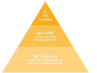
See „Catena X PCF rulebook based on ISO standards“.
The path to sustainability in the semiconductor industry is a collaborative effort that requires commitment from all stakeholders. Together, we can create a more sustainable future! 💯